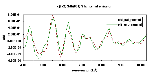
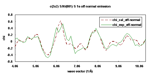
We performed a simultaneous fitting for both normal and off-normal photoelectron diffraction energy scanning curves taken from the Sulfur 1s core-level initial states of Ni(001)+c(2x2)-S. These two ARPEFS measurements were obtained on beamline 3-3, a soft x-ray double crystal monochromator, at Stanford Synchrotron Radiation Laboratory by Barton et al. at room temperature. The first one is a normal emission curve, which used normal emission with the polarization vector inclined 30° from the normal in a [100] direction. The second is an off-normal emission curve, with both emission and polarization vectors aligned with a bulk [011] axis, making an angle of 45° with the surface normal. The instrumental aperture half-angle is about 3°. The Ni(001) substrate has an fcc structure with lattice constant 3.52 Å. The overlayer Sulfur atom occupies a four-fold hollow adsorption site.
Both curves are fit simultaneously with a 83-atom cluster using the three step fitting process (net search, Simplex Downhill, and Marquardt methods). The multiple scattering order is set to 8, the Rehr-Albers approximation order set to 2, and pathcut is set to 0.01. We chose four fitting parameters: the inner potential, the Debye temperature, the spacing between first and second (S-Ni) layers, and the spacing between the second and third (Ni-Ni) layers. Figures 15 and 16 show the best-fit calculated curves (dashed lines) for both experimental curves (solid lines). The fitting procedure gives an inner potential of 10.65 eV, a Debye temperature of 430 K, a spacing between first and second (S-Ni) layers of 1.31 Å, and a spacing between second and third (Ni-Ni) layers of 1.84 Å.
|
|
| Fig. 15. Numerical simulation (dashed line) of experimental photoelectron diffraction scanned energy curve (solid line) for Ni(001)+c(2x2)-S/S1s in the surface normal exit direction. |
|
|
| Fig. 16. Numerical simulation (dashed line) of the experimental photoelectron diffraction scanned energy curve (solid line) for Ni(001)+c(2x2)-S/S1s in 45° off-normal exit direction. |
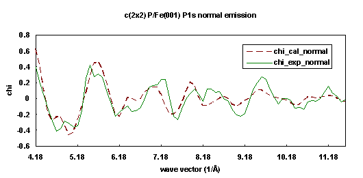
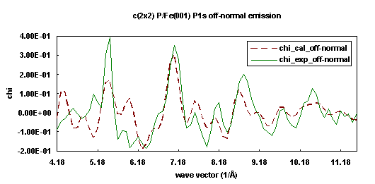
The experiments were performed in an ultra-high vacuum chamber using beamline 3-3, a soft x-ray double crystal monochromator, at Stanford Synchrotron Radiation Laboratory. The photoemission data were collected from the P 1s core level of Fe(001)+c(2x2)-P in two different experimental geometries at room temperature. In the first data set, the photoemission angle was normal to the Fe(001) surface, and the photon polarization vector was 35° from the surface normal. This geometry gives information which is most sensitive to the Fe atoms directly below the P atoms. The second set of photoemission data was collected along the [011] direction, i.e. 45° off normal toward the (011) crystallographic plane, and the photon polarization vector was oriented parallel to the emission angle. By taking ARPEFS data off normal, the structure sensitivity parallel to the surface is enhanced. Analyzed together, the two different experimental geometries allow for an accurate determination of interlayer spacings, bond lengths, and bond angles.
The Fe substrate has a bcc structure with lattice constant 2.87 Å. A simultaneous fitting technique indicates that the P atoms adsorb in the high-coordination four-fold hollow sites. Figures 17 and 18 show the comparison of calculated curves (dashed lines) and experimental curves (solid lines). The P atoms were determined to bond 1.02 Å above the first layer of Fe atoms. The Fe-P-Fe bond angle is thus 140.6°. Assuming the radius of the Fe atoms to be 1.24 Å, the effective P radius is 1.03 Å. The inner potential was found tobe 15.0 eV. It was also determined that there is no relaxation of the first or second Fe-Fe interlayer spacings from the bulk value of 1.43 Å. To test this fitting method, each data set was fit individually and these results were in good structural agreement.
|
| Fig. 17. Numerical simulation (dashed line) of the experimental photoelectron diffraction scanned energy curve (solid line) for Fe(001)+c(2x2)-P/P1s in the surface normal exit direction. |
|
| Fig. 18. Numerical simulation (dashed line) of the experimental photoelectron diffraction scanned energy curve (solid line) for Fe(001)+c(2x2)-P/P1s in 45° off-normal exit direction. |
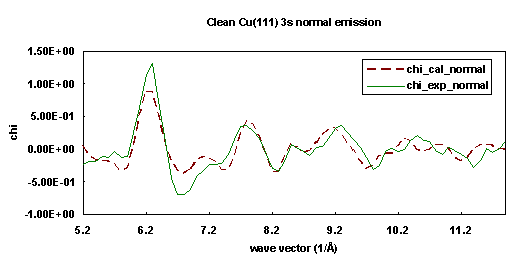
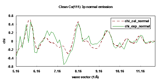
The experiments were performed using the Advanced Light Source at Lawrence Berkeley National Laboratory on beamline 9.3.2 with a soft x-ray spherical grating monochromator. The data were collected using an angle-resolving electrostatic hemispherical electron energy analyzer which is rotatable 360° around the sample's vertical axis and 100° around the sample's horizontal axis. The angle of incidence of the light on the crystal was oriented 80° from the surface normal. The photon polarization vector was thus oriented 10° from the surface normal. The crystal was cooled to about 80K throughout the data collection. Photoemission data were taken from the clean Cu(111) 3p core level and subsequently the 3s core level. The two data sets were acquired in normal exit direction within a few hours of each other.
The fitting procedures were appied to a 77-atom cluster Cu(111) surface separately for the 3s and 3p initial states. The R-factor was minimized as a function of emission angle qe and fe. For the Cu(111) 3s fitting, the R-factor minimum is rather shallow in the range 0° < qe < 5°. However, for qe > 5°, the R-factor rises sharply. In contrast, the Cu 3p R-factor minimum is very steep away from the minimum at qe = 5°. This result indicates that the detected intensity distribution of Cu 3s photoemission is less directional than that of Cu 3p photoemission. Because the emission angle difference of 1° is so important, great care must be taken during the alignment of the experimental system, and also, the modeling must search angle-space to finally obtain the optimum fit to the data. In this case, the emission direction was optimized at 5° off-normal toward the [111] direction. The fitting process for each curve determined that the spacing between first and second layer is 2.06 Å, slightly contracted from the bulk value, 2.09 Å, which agrees with the previous LEED studies. Figures 19 and 20 show the experimental data (solid lines) and their best-fit simulation (dashed lines).
|
| Fig. 19. Numerical simulation (dashed line) of the experimental photoemission diffraction scanned energy curve (solid line) for clean Cu(111) 3s in the surface normal exit direction. |
|
| Fig. 20. Numerical simulation (dashed line) of the experimental photoemission diffraction scanned energy curve (solid line) for clean Cu(111) 3p in the surface normal exit direction. |
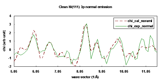
The experiment was performed at the National Synchrotron Light Source at Brookhaven National Laboratory on beamline U3-C, a soft x-ray beamline with a five meter extended range grasshopper monochromator having a fixed exit geometry. The angle of incidence of the light on the crystal was 55° from the surface normal away from the crystal (011) plane. The photon polarization vector was thus oriented 35° from the surface normal and perpendicular to the crystal (011) plane. The analyzer was oriented normal to the Ni(111) surface and the crystal was cooled to about 100K throughout the data collection.
The fitting was done with a 74-atom cluster representing the clean Ni(111) surface. The R-factor was minimized as a function of emission angle qe and fe, which gave an optimized emission direction of 5° off normal. The spacing between the first two layers was found to be 2.06 Å, a slight expansion of the bulk value, 2.03 Å. Figure 21 campares the experimental curve (solid line) and its best fit simulation (dashed line).
|
| Fig. 21. Numerical simulation (dashed line) of the experimental photoemission diffraction scanned energy curve (solid line) for clean Ni(111) 3p in the surface normal exit direction. |
| Return to Van Hove home page |
|---|